Accredited testing laboratory for scanning electron microscopy (SEM) in combination with EDX analyses


Exact characterization and analysis of topography, morphology and pinpoint analysis of chemical elements of materials and components are prerequisites for optimization and quality assurance of products and processes. Scanning electron microscopy (SEM) as well as energy dispersive X-ray spectroscopy (EDX) are particularly well suited to evaluate, for example, fracture surfaces or elemental compositions in the micrometer range. Whether in mechanical engineering, the food industry or medical technology - as a testing laboratory accredited to DIN EN ISO/IEC 17025, we offer independent materials testing and thus support you in optimizing your products.
Our electron microscopes enable the examination of surfaces, microstructures and the analysis of chemical elements
In scanning electron microscopy (SEM), the surface to be analyzed is scanned with a finely focused electron beam. The electrons interact with the atoms of the sample at the surface. The energy emitted is detected by detectors and converted into image values. This enables us to obtain high-resolution images of the microstructures of a surface with high depth of field. A resolution of about 3nm is achieved, so that structures in the nanometer range can be imaged.
For deeper investigations, an SEM with Focused Ion Beam (FIB) is available at our institute. This allows insights under the surface in the micrometer range. In a two-beam arrangement, an ion beam is used to ablate material, allowing a view of the cut surface into the volume.
All our electron microscopes are equipped with a backscatter electron detector and an EDX detector. With the help of the backscatter detector (BSD) a representation of the material contrast is obtained, because heavy elements cause a higher intensity of the backscatter electrons than light elements. Accordingly, the areas of heavier elements in the images appear brighter than the areas of lighter elements. These images can thus be used to draw conclusions about the lateral distribution of different materials or elements in the sample under study.
Energy dispersive X-ray spectroscopy (EDX) on the SEM can be used to determine very precisely the elemental composition of materials on the micrometer scale. The principle is based on the fact that each chemical element emits a characteristic X-ray radiation when excited. All elements of the periodic table starting with carbon can be determined. The EDX systems allow point measurements, area measurements and the measurement of element concentrations on a defined area or along a line (mappings and linescans).
Our different electron microscopes complement each other perfectly with regard to their specifications, so that we can support you in a wide variety of problems:
- Fracture surface investigations
- Surface topography investigations
- Layer thickness measurements
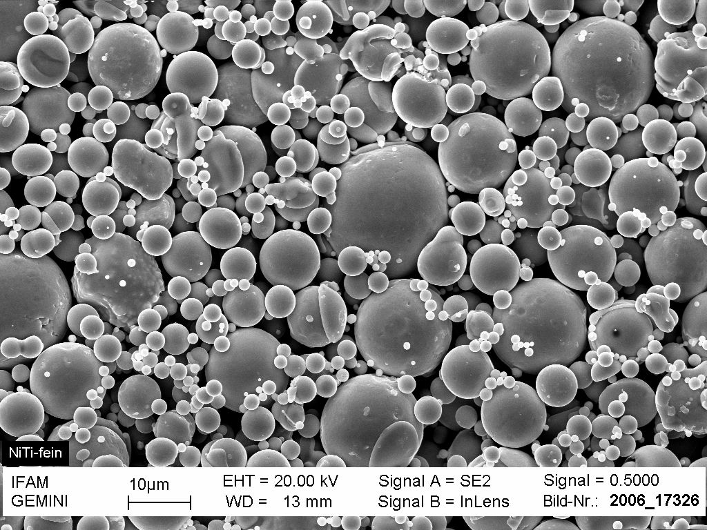
- Powder investigations (also nano-powders)
- X-ray microanalysis (EDX): mappings (area analyses), linescans (line analyses), spots (point analyses)
- Ion beam etching (FIB)
- FIB/REM investigations also under cryo-conditions
Material analyses for research, development and industry
The application possibilities of scanning electron microscopy in combination with energy dispersive X-ray microanalysis are vast. Practically all solids such as metals, plastics, ceramics and glass can be analyzed. In addition, samples that are in the form of particles, powders or adhesions can also be examined.
Here are a few concrete examples of the use of our materials testing by SEM and EDX: