Printed conductive structures made of special alloys
Fraunhofer IFAM has the expertise and equipment to produce printable metal and alloy inks for special applications. These inks made from special alloys for digital printing techniques offer opportunities for cost-efficient new products in the field of printed electronics and sensor technology in a wide range of industries.
Development of printable inks and pastes
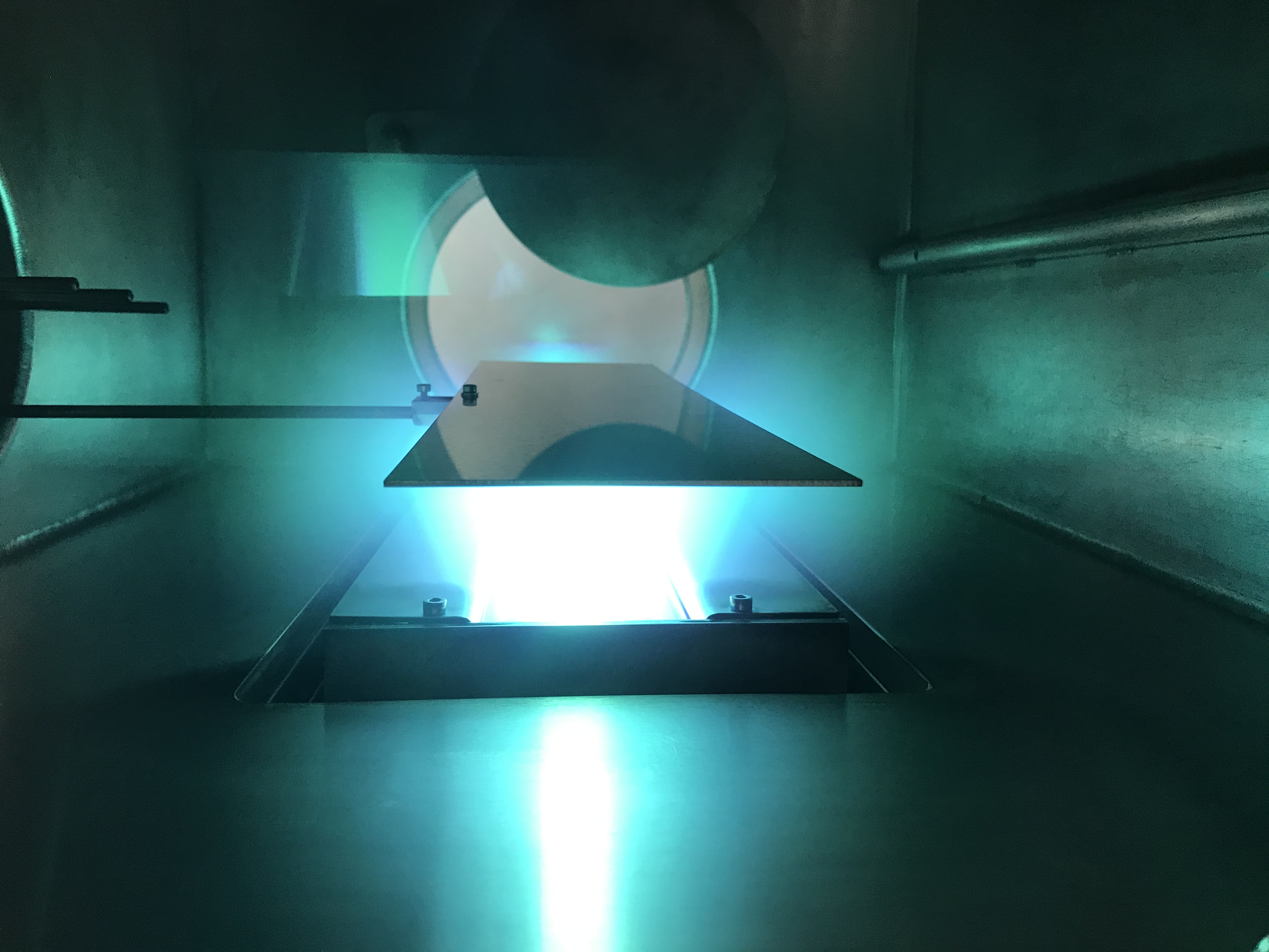
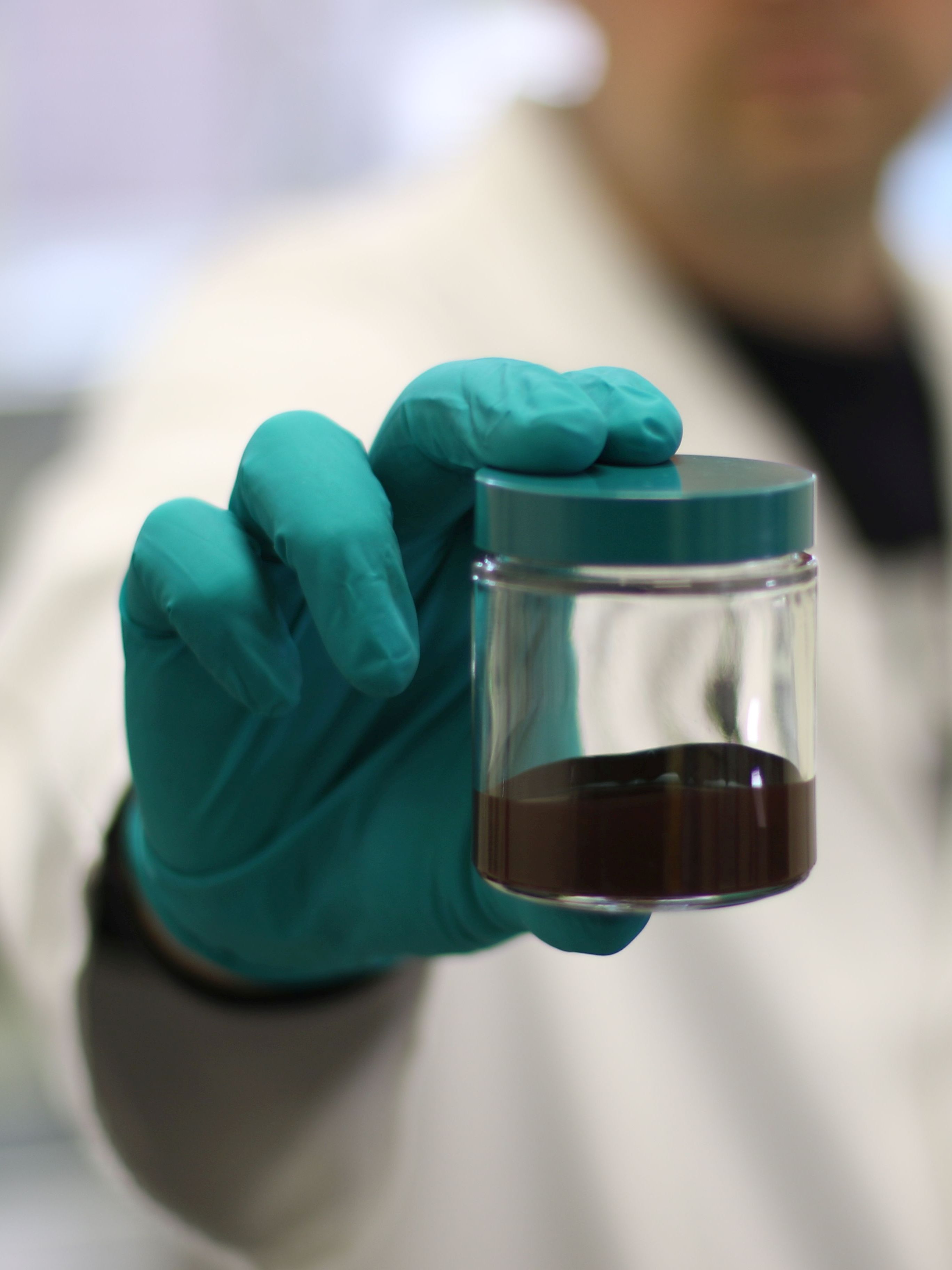
One possibility for the physical production of printable alloy inks is a chemically pure deposition of metals or metal alloys from the gas phase into printable liquids. Physical vapour deposition of metallic materials and alloys, also known as "sputtering", is carried out at Fraunhofer IFAM using a variant of the so-called VERL process (Vacuum Evaporation on Running Liquids), which is used to produce nanodispersions in silicone oil or diethylene glycol (DEG). In this process, nanoparticles are deposited directly from the gas phase into liquid media.
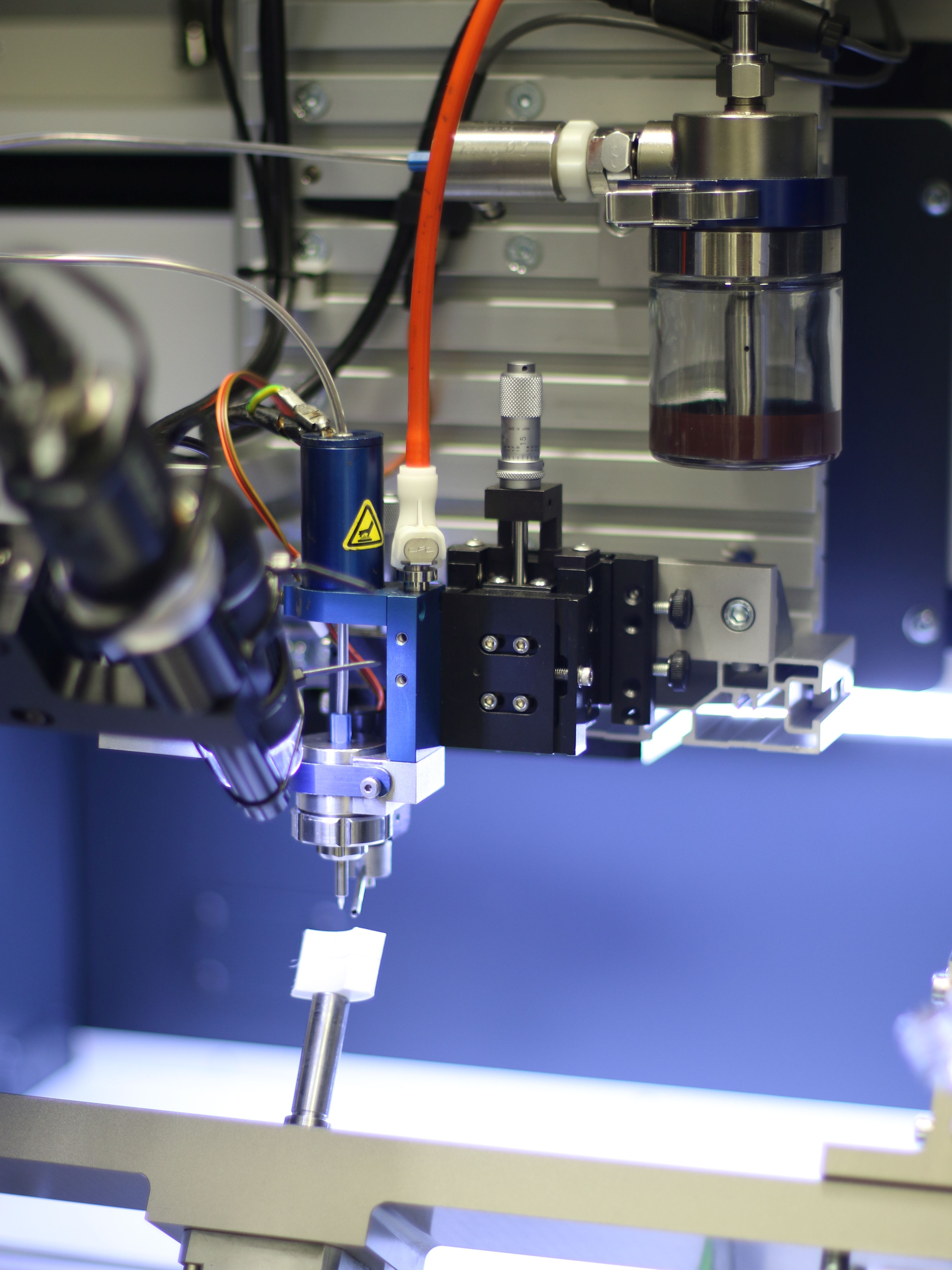
These nanoscale dispersions can be used to produce functional metal inks or inks made from special alloys, which can be printed using digital printing technologies such as inkjet and aerosol jet printing. Compared to mask-based processes such as lithography or screen-printing, digital printing technologies have the advantage that layouts can be created and changed more easily. This also enables the efficient production of small quantities of individualised products as well as rapid product development. Additive methods also have better resource efficiency and are more environmentally friendly than subtractive processes; in particular, aggressive chemicals can be avoided, such as hydrofluoric acid in etching processes.
The printed structures are structurally compressed and made electrically conductive by an efficient sintering process. In addition to thermal processes, photonic sintering processes are also suitable for this purpose. These photonic processes also enable the processing of oxidation-sensitive inks and post-treatment on substrates with limited temperature resistance, which include many standard thermoplastics such as polymethyl methacrylate (PMMA), polystyrene (PS), polycarbonate (PC) or polyethylene terephthalate (PET).
Wide range of applications for printed components and sensors
These plastics are widely used in many industries such as packaging, automotive and medical technology and offer great potential for functionalised low-cost devices. These plastics also play a major role for optically transparent components.
Besides metallic inks, special alloy inks in particular are helping to open up new areas of application for printed components or sensors in various industries. Alloy inks made of CuNiMn can be used as printed strain gauge structures on various substrates in a wide range of applications. Printed heating structures can be used for local heating of surfaces in automotive applications, in chemical processes, in biotechnology, in medical technology or in gastronomy. Printable alloy inks allow the realisation of printed functional structures on multifunctional PCBs or on ultra-thin film-based flexible microsystems with embedded flat components. Also generatively manufactured ("3D-printed") or injection-moulded components can be equipped with additional functionalities with the help of the innovative alloy inks. The innovative alloy inks developed at Fraunhofer IFAM thus contribute significantly to the currently fast-growing research field of 3D electronics.
Metal alloys for printed electronics
In the growing market of printed electronics, the demand for metallic inks and pastes is continuously increasing. In addition to precious metals such as silver (e.g. for conductors) and gold (e.g. medical technology applications), printable metal alloys (e.g. CuNiMn) are needed for strain and temperature sensors, for heating structures or for high-precision printable resistors.
For digital printing technologies, inks made from special alloys therefore offer the opportunity for affordable new products in the field of printed electronics and sensor technology in a wide range of industries. This offers particular advantages for small batch sizes and thus also for personalised products, because with digital printing techniques the layouts can be designed on the computer with little effort and printed immediately. In addition, in contrast to mask-based processes such as lithography or screen-printing, layout changes can be implemented within a short period of time without major effort, which enables rapid customisation of product features. The research results of Fraunhofer IFAM enable companies along the entire value chain from the fields of ink production, plant engineering, microsystems technology, electronics, sensor technology or printed circuit board technology to expand their product portfolios and thus expand existing or open up new business areas.
 Fraunhofer Institute for Manufacturing Technology and Advanced Materials IFAM


